


Work Function Tuning for Metal Gate Transistors
Throughout the integrated circuit technology development over the past forty years, complementary metal-oxide-semiconductor field-effect transistor (CMOSFET) device technology has been the dominant very large scale integrated (VLSI) technology. The scaling rules for CMOS device were originally predicted by Gordon Moore in 1965, and since then it has been the driving force for the improvement of speed and shrinkage of chip area of integrated circuits. MOSFET device dimensions continue to be aggressively scaled to satisfy the high demand for improving circuit performance with decreased power and increased integration density. Continuation of scaling rules have eventually reached fundamental limits of both materials and devices currently being used in CMOS devices [1-3]. Maria in her term project have discussed in detail about the electronic devices & main principles for the operation of transistors [4].
The reduction of gate oxide thickness is necessary to maintain device scaling, including threshold voltage and capacitance. An equivalent gate oxide thickness (EOT) of less than 1nm is needed for high performance device. However, it appears that the fundamental limit of the CMOS process will be reached in the near future and quantum mechanical effects need to be considered. As device size decreases, gate leakage current increases rapidly due to direct tunneling. In addition, gate control reduces and poly-silicon boron penetration effect into the channel becomes significant for PMOSFETs. Since SiO2 and poly-silicon materials face fundamental issues for scaled devices, alternative materials are necessary to continue scaling. To achieve low EOT, and stable gate electrode characteristics, both high dielectric constant (k) oxides and metal gate electrodes have considered necessary for advanced devices [5-6]. Hafnium oxide looks to be viable replacement for SiO2 having a high dielectric constant of 25 compared to 3.9 of SiO2. Figure 1 shows the static dielectric constant (k), experimental band gap and (consensus) CB offset on Si of the candidate gate dielectrics and static dielectric constant versus band gap for candidate gate oxides. [5]
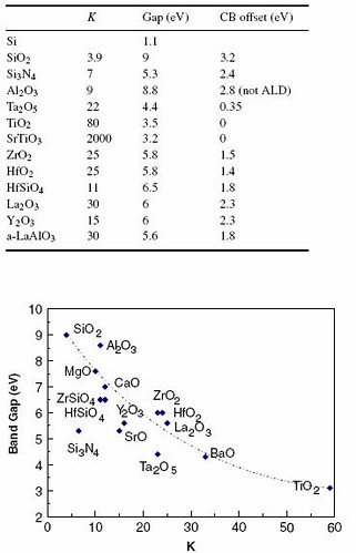
Figure 1: Static dielectric constant (k), experimental band gap and (consensus) CB offset on Si of the candidate gate dielectrics and static dielectric constant versus band gap for candidate gate oxides.
Candidates for new metallic gates have many requirements which include appropriate work functions, good thermal/chemical interface stability with underlying dielectric and high carrier concentration and process compatibility with current and future CMOS. A desirable metal gate should have an appropriate work function for NMOS or PMOS devices. This implies a work function of ~4eV for NMOS devices and ~5eV for PMOS devices. Dual metal gates or midgap metal gate electrodes can be used in CMOS processing however with a more complex process integration scenario. Midgap work function metal gates, which are being considered due to their ease of integration, will most likely not be suitable for scaled bulk CMOS devices due to a high resulting threshold voltage which cannot be reduced simply by lowering the substrate doping since the channel doping will then become too low to control short-channel effects. For this reason, two different gate metals are required with work functions near the conduction and valence band edges of Si. It should also have good thermal stability with the underlying dielectric, signifying that the choice of high k dielectric is vital from a metal processing standpoint. In addition, a low diffusivity to oxygen and other dopants of the metal gate is necessary. Furthermore, candidate metals should have high carrier concentration so that gate depletion effects are negligible. Much investigation is ongoing concerning alternative metal gate electrodes including elemental, nitrides, silicides, and alloys [7-9]. First principle calculations using DFT are being performed to study the work functions to achieve the above stated. Satyesh in his term project discussed about the application of DFT [10]. Now we will look at the basics of work function.
Work Function in Metals
If we heat any metal at high enough temperature, we can give the electrons sufficient energy to overcome the natural barrier that prevents them from leaking out from its surface. This phenomenon is known as thermionic emission. This property is employed in vacuum tubes, in which the metallic cathode is usually heated in order to supply the electrons required for the operation of the tube [11]. Another way to get the electrons leak out is by field emission. Field electron emission also known as field emission is a phenomenon involving the electric field induced emission of electrons from the surface of a condensed material (either solid or liquid), into vacuum or into another material. Both thermionic and field emission sources are used for the generation of electron beam in electron microscopes. Williams and Carter in their book on Transmission electron microscopy discussed about the electron sources in Chapter 5 [12].
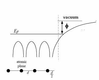
Figure 2: Schematic energy diagram for metals, showing the work function.
Figure 2 shows a schematic energy diagram of a metal. The valence bands are filled with electrons up to the Fermi energy (EF). The distribution of electrons among the levels is usually described by the distribution function f(E) which is zero when EF < E and is 1 EF > E at 0 K, however the distribution function at T not equal to zero is given by Equation 1, which is known as Fermi-Dirac distribution is shown schematically in Figure 3. The energy difference between Fermi energy and vacuum level corresponds to the work function ($\phi$). The work function corresponds to the minimum amount of energy needed to remove an electron from the metal. In metals, work function and ionization energy are the same [13].
(1)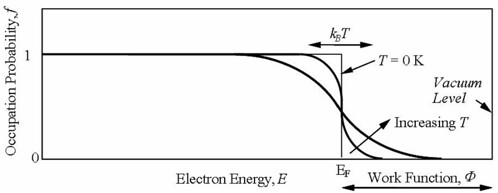
Figure 3: The distribution function f(E) at T = 0 K and T > 0 K
The work function of a surface is strongly affected by the condition of the surface. The presence of minute amounts of contamination (less than a monolayer of atoms or molecules), or the occurrence of surface reactions (oxidation or similar) can change the work function substantially. Changes of the order of 1 eV are common for metals and semiconductors, depending on the surface condition. These changes are a result of the formation of electric dipoles at the surface, which change the energy an electron needs to leave the sample. Due to the sensitivity of the work function to chemical changes on surfaces, its measurement can give valuable insight into the condition of a given surface. The work function also has significant influence of the band line-up at semiconductor interfaces and this will be discussed in the next section.
Work function depends on the surface orientation (anisotropy of work function), this can be seen in Table 1 and Table 2. For a crystal with N electrons, if EN is the initial energy of the metal and EN-1 that of the metal with one electron removed to a region of electrostatic potential Ve, we define work function as
(2)At 0 K, the chemical potential ($\mu$) by definition is
(3)In the limit of large systems, all polarisation effect can be neglected after removing the electron. Then chemical potential is then shown to coincide with the Fermi energy. The work function, finally, is the difference between the Fermi level and the vacuum level.
(4)The calculation of work function is then divided into two parts. First is to perform a self-consistent calculation to find the Fermi energy of the slab. Second, we need to find the electrostatic potential in the vacuum level. The electronic density n(r) is the basic variable calculated by DFT. Introduce the plane-averaged electronic density:
(5)where z axis is perpendicular to the slab surface S. The macroscopic-average electronic density $\widehat{n}$ is then defined from the integration over the interplanar distance d of the slab:
(6)The potential is related to the charge density via the Poisson equation. So we can get a similar relation between plane-averaged potential $\overline{V}_{e}$(z) and macroscopic average $\widehat{V}_{e}$(z).
(7)By plotting the macroscopic average over the z axis, the vacuum level is found. Because the curve of the average is nearly flat in the vacuum provided the vacuum is large enough. Subtracting this vacuum level from the Fermi level gets the work function for the metal surface. This can be seen in the Figure 4.
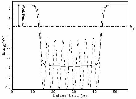
Figure 4: Subtracting this vacuum level from the Fermi level gets the work function for the metal surface.
Slab model is the most popular way to model the surface.The slab model consists of a film formed by a few atomic layers parallel to the crystalline plane of interest.Using plane waves needs to force a 3-D periodicity. The thin slabs needs to repeat in one direction. To perform a supercell calculation, one defines a unit cell oriented with one axis perpendicular to the surface of interest, containing the inequivalent atoms of a crystalline thin film and some vacuum layers. Ideally, the thickness of the vacuum layer and of the slab must be large enough for two successive metal surfaces not to interact significantly and such a slab can be seen in Figure 5. It is not trivial to construct the slab model at first. You need to visualize them and various surfaces of fcc is shown in Figure 6. It is to be noted that surface primitive cell is two-dimensional, is different from conventional bulk primitive cell.

Figure 5:Typical model of the slab used for calculations
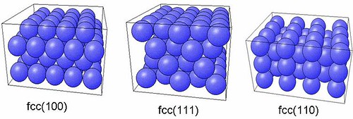
Figure 6:Various fcc surfaces used for the calculations
A recipe for DFT calculations (of course proper cut off energy for the plane wave expansion, ultra-soft psuedo potentials, proper k-point mesh, proper size of the slab, proper exchange correlation approximations and good soft ware package should be used) of work function is as follows
- As a preliminary step towards the study of surface, we have to find the equilibrium lattice constant.
- It is well known that the equilibrium atomic positions in a crystal surface are generally different from those in the ideal bulk-terminated surface. We need to perform a relaxation calculation to find the equilibrium geometry of the surface.
- The relaxed coordinates are put into another input file to perform a self-consistent calculation to find the Fermi energy in the slab
- Using post-process code to extract the electrostatic potential from the output file.
- Calculate the macroscopic average potential to determine the vacuum level.
- Put the two values into the definition of the work function to determine the final solution.
Summary of such calculations for Al and Cu are shown in Table 1 and Table 2 respectively. The results shows a little deviation from the experimental values. It may be due to the experiment is performed at room temperature, while the DFT calculation is at 0 K. Overall, it shows good accuracy using this method since the error is within the computational range. From the Cu, we see that it shows the trend (110), (100),(111) of increasing work function. This is best explained by the Smoluchowski [14] smoothing. This smoothing leads to a dipole moment which opposes the dipole created by the spreading of electron and thus reducing the work function. Surface orientations of high density experience small smoothing, inducing a small reverse dipole, and thus a high work function. However, from the calculation, it is seen that the Al doesn’t obey this increasing ordering. In the paper by Fall, C. J. et al., , [15] the authors investigated this phenomenon and concluded that the trend of the work function Al can be explained by a charge transfer the atomic-like p orbitals of the surface ions perpendicular to the surface plane to those parallel to the surface, when compared to the bulk charge density. Thus it results from a dominant p-atomic-like character of the density of states near the Fermi energy. Overall, the DFT calculations recovered both the normal and abnormal anisotropy of the work function of the fcc metals.
| Al | Fermi Level (eV) | Vacuum (eV) | Work Function (eV) | Experimental (eV) |
| (100) | 2.364 | 6.782 | 4.418 | 4.41 $\pm$0.02 |
| (110) | 2.488 | 6.768 | 4.28 | 4.28 $\pm$0.02 |
| (111) | 2.634 | 6.869 | 4.235 | 4.24 $\pm$0.03 |
Table 1: Calculations of work functions of Aluminum, showing that work function is dependent on the type of surface
| Cu | Fermi Level (eV) | Vacuum (eV) | Work Function (eV) | Experimental (eV) |
| (100) | 5.551 | 10.391 | 4.84 | 4.59 $\pm$0.03 |
| (110) | 2.390 | 7.105 | 4.715 | 4.48 $\pm$0.03 |
| (111) | 5.581 | 10.780 | 5.199 | 4.94 $\pm$0.03 |
Table 2: Calculations of work functions of different surfaces of Cu.
In thermionic emission source in TEM, the filament or the source is usually tungsten and LaB6 which are grown with <110> orientation to enhance emission and to get high current density. Field emission, like thermionic emission from LaB6 depends on crystallography of the tungsten tip, the <310> orientation is found to be the best. Thus a study of work function from different surfaces is very important to achieve desired properties [12].
The work function is intimately related to the dipole barrier at the surface, and has been equated to the electronegativity in the case of elemental crystals (the electronegativity being the ability of one element to compete with others for the valence electronic charge during compound formation). It is also well known that adsorption of species at a surface alters the work function of the surface in an understandable manner, with adsorbates having higher electronegativities than the surface increasing the work function while those with lower electro negativities having the opposite effect. R. Ramprasad et al., quantified these anticipated trends for the test case of graphene ribbon edges with various adsorbates [16]. The article by H. B. Michaleson on "the work function of the elements and its periodicity" indicates how this behavior not only permits successful prediction of the work function of unmeasured elements but also defines certain trends of data. As in the case of many physical properties, these trends and sequences in the periodic table are most useful for comparing and evaluating data and for planning research [17]. Figure 7 shows the periodic system of elements, with work function in eV. Data are for polycrystalline specimens. Figure 8 shows the relation of experimental values of the work function to the periodic system of the elements. Solid line correspond to rows in the table of the elements and dashed lines to columns [17].
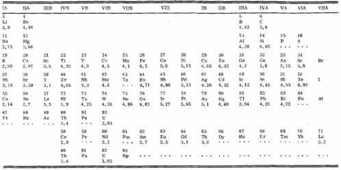
Figure 7: Periodic system of elements, with work function in eV. Data are for polycrystalline specimens.
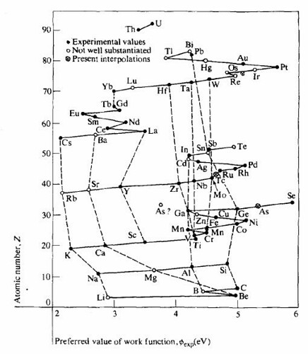
Figure 8: Relation of experimental values of the work function to the periodic system of the elements. Solid line correspond to rows in the table of the elements and dashed lines to columns.
Measurement of Work function
Many techniques have been developed based on different physical effects to measure the electronic work function of a sample. One may distinguish between two groups of experimental methods for work function measurements: absolute and relative. Methods of the first group employ electron emission from the sample induced by photon absorption (photoemission), by high temperature (thermionic emission), due to an electric field (field electron emission), or using electron tunnelling. All relative methods make use of the contact potential difference between the sample and a reference electrode. Experimentally, either an anode current of a diode is used or the displacement current between the sample and reference, created by an artificial change in the capacitance between the two, is measured (the Kelvin Probe method, Kelvin probe force microscope).
Photoelectron emission spectroscopy (PES) is the general term for spectroscopic techniques based on the outer photoelectric effect. In the case of Ultraviolet Photoelectron Spectroscopy (UPS), the surface of a solid sample is irradiated with ultraviolet (UV) light and the kinetic energy of the emitted electrons is analysed. As UV light is electromagnetic radiation with an energy hf lower than 100 eV it is able to extract mainly valence electrons. Due to limitations of the escape depth of electrons in solids UPS is very surface sensitive, as the information depth is in the range of 2–20 monolayers (1-10 nm). The resulting spectrum reflects the electronic structure of the sample providing information on the density of states, the occupation of states, and the work function [18]. There are other methods also available based on thermionic emission.
Field Emission and Tunneling
When a small field is applied there is a lowering in the energy barrier and results in field emission which is shown in Figure 9. Due to the image force and electric field the effective work function is
The current density (J) is given by the expression below and is known as the Schottky effect or barrier lowering effect and if there is no barrier lowering it is purely thermionic and the expression takes Richardson-Dushman equation form. Experimental verification can be done by a plot of log (J/T2) vs 1/kT, which gives a straight line with a slope and with which we can get the work function.
(9)The presence of an electric field increases the emission current due to barrier lowering. Further increase in electric field (~109 V/m) leads to electrons tunneling through the potential barrier as shown in Figure 9 (The barrier becomes thin under the electric field and the electrons can tunnel through–field emission). This is called Fowler-Nordheim tunneling effect. The tunneling current is given by the expression
(10)Here the plot of ln(JFN/(V/d)2) vs 1/(V/d) gets us the work function [19-20]
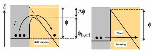
Figure 9: Field emission by applying a small electric field and tunneling by a large field
Work Function in semi conductors
Figure 10 shows a schematic energy diagram of a n-type semiconductor. Valence bands and conduction bands are separated by the band gap (Eg). In a nondegenerate semiconductor (having a moderate doping level), the Fermi level is located within the band gap. This means the work function is now different from the ionization energy (energy difference between valence bands maximum (VBM) and vacuum level). In a semiconductor, the Fermi level becomes a somewhat theoretical construct since there are no allowed electronic states within the band gap. This means the Fermi distribution needs to be considered, which is a statistical function that gives the probability to find an electron in a given electronic state. The Fermi level refers to the point on the energy scale where the probability is just 50%. Even if there are no electrons right at the Fermi level in a semiconductor, the work function can be measured by photoemission spectroscopy(PES). For summary of doped semiconductors in electronic devices refer to Maria's term paper [4].
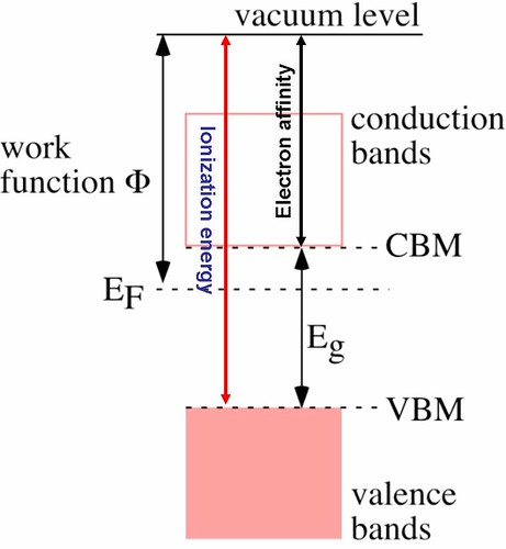
Figure 10: Schematic energy diagram in an n-type semiconductor
Figure 11 shows the n-type semiconductor junction to a metal on the left and a p-type semiconductor junction to a metal on the right. In an n-type semiconductor junction to a metal, Fermi level of semiconductor is above that of metal, so upon contact electrons go from semiconductor to metal, the barrier height and the build in potential is given by the equations
(11)In an p-type semiconductor junction to a metal, Fermi level of semiconductor is below that of metal, so
upon contact electrons go from metal to semiconductor. The barrier height and the build in potential is given by equations
The “built-in” potential is sometimes referred to as the “band-bending”, as it is the amount that the VB and CB change by in going from the bulk to the interface. The built-in potential controls the length scale of the semiconductor depletion region, and also control the barrier that electron see in going from the semiconductor to the bulk. The “barrier height” is the total barrier from the Fermi level of the metal to the
conduction band (for n-type semiconductors) or valence band (for p-type semiconductors) [19-20]. Table 3 gives a summary of barrier heights for metal-semiconductor junctions.
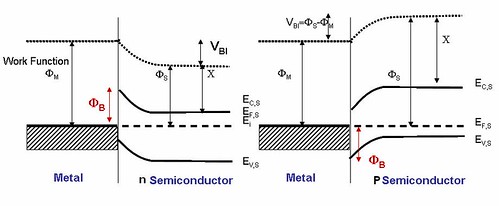
Figure 11: n-type semiconductor junction to a metal and a p-type semiconductor junction to a metal
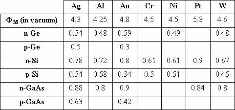
Table 3: Barrier Heights for metal-semiconductor junctions
Conclusions
The work function of a crystal surface is defined as the energy needed to remove an electron at the Fermi level from the bulk region of a crystal to the vacuum at infinity. Apart from describing the ability of an electron to escape from a material, it correlates with the chemistry at the surface of a crystal. Study of work functions of various materials theoretically and experimentally can be much useful to develop new electronic devices.


